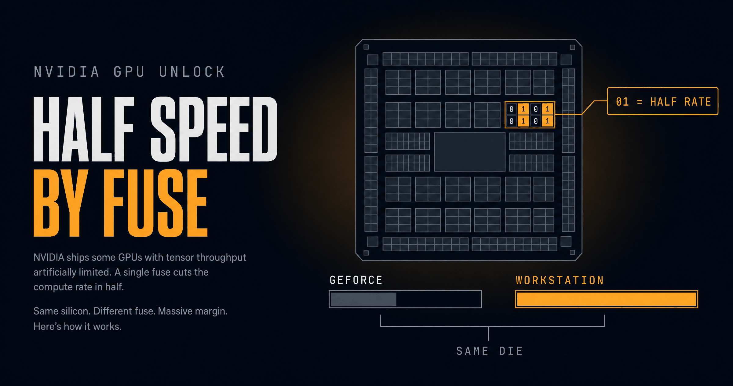
The RTX 4090 and the RTX 6000 Ada come off the same AD102 die. One costs $1,599 and the other $6,800, and part of what you’re paying for is a single value burned into a fuse: full rate instead of half rate on the math that every AI workload depends on. The 3090 Ti and the A6000 are the cleaner example, since those two match core for core, 84 SMs each, at $1,999 and $4,650.
In October, a Linux kernel module started flipping that value on consumer cards. RTX 4090 owners watched their measured tensor instruction rate go from 165.6 to 331.6 TFLOPS. RTX 3090 Ti owners saw BF16 matrix math jump 80%. RTX 2080 Ti owners got their card’s full tensor rate back, seven years after they bought it.
The benchmark numbers are real. What they mean for your actual workload is smaller than the headlines suggest, and that gap is the interesting part.
What FP32 accumulation is, and why AI math lives on it
A matrix multiply is a chain of multiply-and-add operations. The multiply inputs can be narrow. The running sum needs room, because you’re adding thousands of products and each addition can drift.
FP16 carries about 3 decimal digits of precision and a narrow exponent range. Accumulate 4,096 products in FP16 and the sum saturates or drifts. Accumulate in FP32, which carries about 7 digits and a much wider range, and the error stays in the noise. So every serious training kernel multiplies in FP16 or BF16 and accumulates in FP32. The “FP32” is not about the weights. It’s about the adder.
That single design choice is why the throttle matters. The tensor core operation f16 × f16 → f32 accumulate is the hot instruction in:
- Training and fine-tuning, every forward and backward GEMM
- LoRA training, which is nothing but GEMMs on a frozen base
- Prefill in LLM inference, where the model processes thousands of prompt tokens at once
- Attention in any precision, since FlashAttention accumulates in FP32
- Diffusion and video DiTs, whose transformer blocks are the same shape
The instruction f16 × f16 → f16 accumulate is a different instruction, and NVIDIA never throttled it. Neither did they throttle FP32 CUDA cores, INT8 tensor math, or NVFP4 on Blackwell.
Where the throttle lives
It isn’t in the driver, and it isn’t in the compiler. It’s in two registers.
FEAT_OVR_SM_SPD at 0x0082381c holds eight 4-bit fields, one per instruction class: double precision, FFMA, FMLA16, FMLA32, and IMLA0 through IMLA3. A second register, FEAT_OVR_SM_SPD_1 at 0x00823820, holds the field for IMLA4. Each field is encoded the same way: bit 3 enables the override, and bits 2:0 pick the rate. 000 is full, 001 is half, 010 is quarter, 011 is eighth.
The documented default on GA102 is 0x00000001. Decode the low nibble and it reads 0001: override off, speed selector 001, half rate. Set all eight fields to full with override enabled and you get the target value 0x88888888.
The registers aren’t writable from the host because a second register guards them. FEAT_OVR_PLM at 0x00823804 defaults to 0xffffff8f. The low byte is a privilege mask: 1111 means all four privilege levels can read, and 1000 in the write nibble means only L3 can write. L3 is the GPU’s heavy-secure context. Your driver runs at L0.
So the unlock has to do two things: raise the mask to 0xffffffff and write the speed values. Both require code running at a privilege level you don’t have.
How the exploit works
It’s a hardware security story that happens to have a performance payoff.
On Turing, Ampere and Ada, the driver starts the GPU by loading a signed firmware image called the Booter onto the SEC2 security processor, a Falcon microcontroller inside the GPU. The Booter verifies and launches the GSP resource manager firmware, and it runs in heavy-secure mode, the same privilege level that can write those registers.
The Booter has a stack buffer overflow. You control the length of a signature blob it copies into a fixed-size stack buffer, and the copy runs past the end, over the stack canary that’s supposed to catch exactly this. Researchers got a return-oriented-programming primitive out of it. Jon Pry’s paper, “A Canary in the Crypto Mine,” documents the class of bug.
Getting the gadgets was easier than it should have been. NVIDIA shipped both debug and production Booter blobs for a while, and the debug image was encrypted with a known public test-key scheme, key index 37. Decrypt it, disassemble it, and you have NVIDIA’s own gadget library to chain. The debug build isn’t byte-identical to production, but it’s close.
The result is a payload that performs one 4-byte write to an arbitrary address, from inside heavy-secure mode, using NVIDIA’s own signed code. Raise the mask, write the rate, reset the card, let the stock driver load. No patched driver, no VBIOS flash.
The whole thing is volatile on purpose. The value lives in the registers, so it survives a PCIe function-level reset and a driver reload, and it’s gone when you power off. That’s why the modules run from the initramfs on every boot, before nvidia binds the card.
It started on mining cards. The CMP 170HX unlock used the same bug to turn the 8 GB and 10 GB variants into 64 GB and 40 GB parts. GeForce ports followed: Turing-unlock as a UEFI loader, Zagitta/gpu-unlock for Ampere as a kernel module, JustAResearcher/gpu-unlock-ada for Ada.
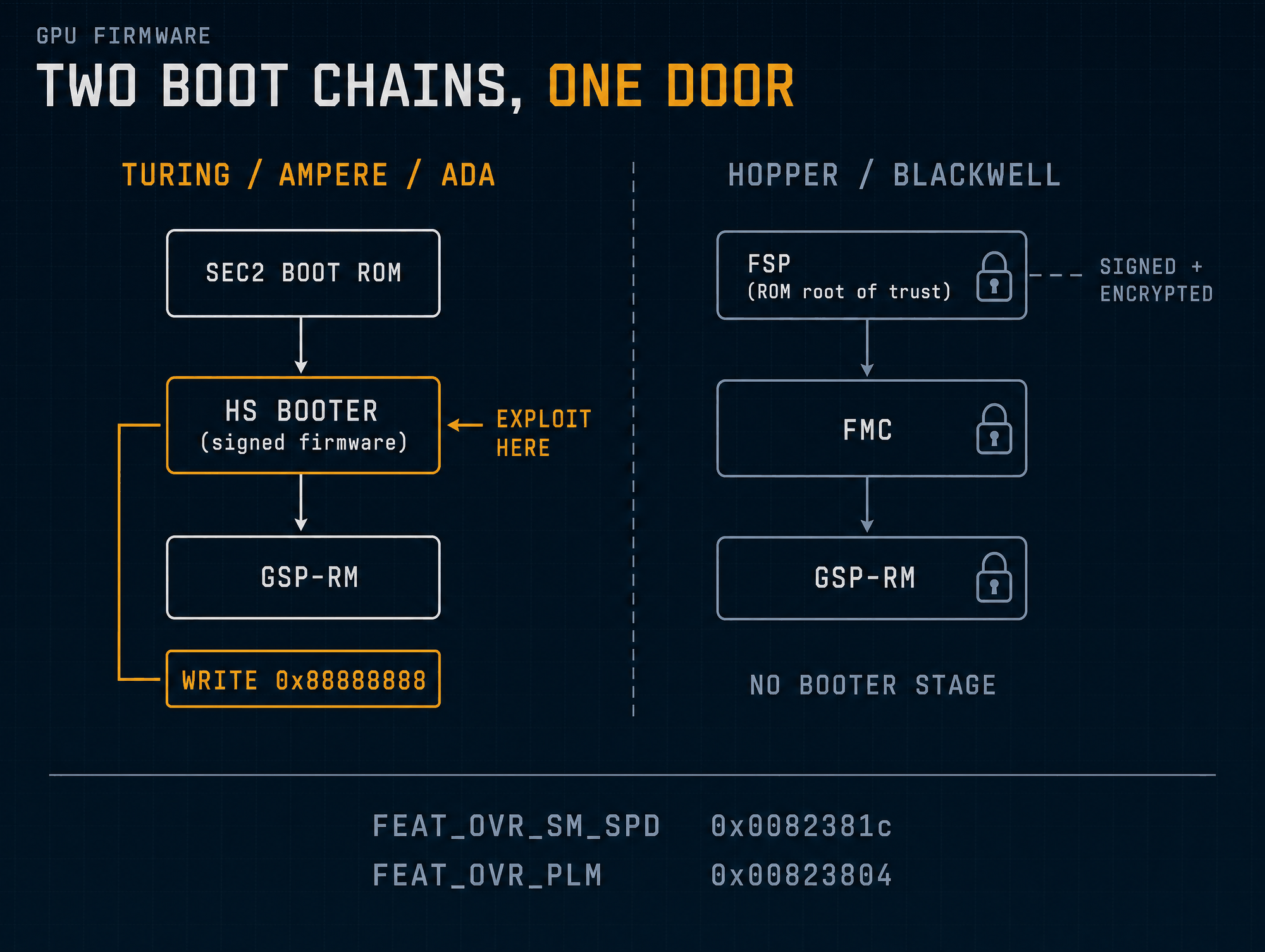
The two boot chains. On the left, a signed firmware stage runs early enough and privileged enough to write the speed registers. On the right, that stage doesn’t exist.
What you actually get
First, the headline number everyone quotes, which is the tensor instruction issue rate on an RTX 4090:
| Mode | Stock | Unlocked |
|---|---|---|
| FP16 → FP32 accumulate | 165.6 TF/s | 331.6 TF/s |
| BF16 → FP32 accumulate | 165.5 TF/s | 330.6 TF/s |
| FP16 → FP16 accumulate | 325.7 TF/s | 331.6 TF/s |
That last row is the control, and it’s the proof the unlock works the way it claims. FP16-accumulate was never throttled, so it barely moves. The first two rows double.
Now the part that matters. The same repos measured cuBLAS GEMMs, which is what your code actually calls:
- FP16 GEMM on the 4090: 12% to 34% faster, depending on shape
- BF16 GEMM on the 4090: 16% to 20% faster, and essentially unchanged at 4096³
- FP16 GEMM on a 3090 Ti at 450 W: 87.46 to 118.39 TFLOPS, up 35%
- BF16 GEMM on the same 3090 Ti: 87.50 to 157.41 TFLOPS, up 80%
- TF32 GEMM on the same card: 42.58 to 82.61 TFLOPS, up 94%
- 2080 Ti: instruction rate 2.00×, cuBLAS GEMM 1.77×
The gap between “2× instruction rate” and “12 to 34% GEMM” is the whole story. Doubling how fast the tensor core accepts an FMA doesn’t double your matrix multiply if the kernel is waiting on memory, launch overhead, or the power limit. Cards that were compute-bound at a given power ceiling gain the most. Cards that were already bandwidth-bound barely move, which is why cards that added 80% on BF16 GEMM still reported about 15% on real LLM prefill.
Community reports fill in the application layer, and they’re consistent with the microbenchmarks:
- LLM prefill, 3090: about 15% faster prompt processing, 5% faster token generation
- LLM prefill, 3080: 2,200 to 2,600 tokens/s
- Long context, dual 3080 20 GB: 11% faster decode at a 256K prompt, because attention dominates there
- LoRA training, 3080 Ti at 300 W: 8 to 10 seconds per iteration down to 4.5 to 7
- Diffusion: mixed. Reports range from nothing to about 20%
- Quantized MoE serving: one 48 GB modded 4090 measured 0.983× on 8K prefill, no gain at all
That last number isn’t a failure. It’s diagnostic. Quantized matmuls that use integer tensor math (INT8 × INT8) never touch the throttled path, so there’s nothing to unlock. llama.cpp leans on integer matmuls, which is a big part of why it shows a smaller gap than vLLM, whose Marlin and AWQ paths dequantize to FP16 and accumulate in FP32.
Where you get nothing
Worth being blunt, because the Reddit threads are full of people benchmarking the wrong thing:
- Token generation at batch size 1. Decode is a memory-bandwidth problem. Even though it executes FP32-accumulate instructions, there aren’t enough of them per byte moved to matter.
- Pure FP32 work on CUDA cores. Never throttled.
- INT8 and INT4 tensor math. Never throttled. INT8 on a 4070 Ti SUPER measured 379.5 TOP/s before and after. Unsigned INT4 stayed at about 754.8 TOP/s in both states.
- NVFP4 on Blackwell. Never throttled, because Blackwell’s FP4 path is new.
- Gaming. No evidence of any effect. If DLSS or frame generation used FP32 accumulation, the penalty on consumer silicon would have been obvious years ago, so they almost certainly don’t. That’s also why the throttle survived unnoticed for so long.
Why Blackwell can’t be unlocked
The fuses are identical. The author of the original writeup checked his own cards: fmla32 reads half rate on a 5090 and full rate on a 6000 PRO, same register map. The difference is the door.
Starting with Hopper, NVIDIA moved the GPU’s root of trust to the FSP, a RISC-V security core that boots from immutable ROM the moment the GPU gets power. The Linux kernel documentation for the new nova driver lays out the change:
On Hopper/Blackwell GPUs, FSP replaces this multi-stage process with a single message-driven interface: FSP (hardware root of trust, boots from ROM) → FMC (Falcon Microcontroller, verified by FSP) → GSP-RM (verified and loaded by FMC). […] There is no SEC2 involvement, no Booter ucode, and no FWSEC-FRTS stage.
No Booter means no stack overflow in a signed, heavily privileged firmware stage. The driver now hands the FSP a firmware hash and an RSA-3K signature and lets the ROM code decide. According to the same writeup, the firmware shipped for Blackwell is encrypted, and unlike Ada there is no public-key debug build to decrypt and mine.
There’s also a design-language shift that makes the class of bug rarer: NVIDIA has publicly described using SPARK, the formally verifiable Ada subset, for critical RISC-V firmware. A verifier that proves the absence of runtime errors is aimed at exactly the kind of memory-safety bug the Booter had.
So the window is Turing, Ampere and Ada. The accepted-device list is 72 PCI IDs across TU102/104/106, GA102/103/104/106, and AD102/103, with published same-card numbers for three of them: RTX 2080 Ti, RTX 4090, and RTX 4070 Ti SUPER. Everything else rests on user reports.
The 4090 is the last flagship that can be unlocked, and if the FSP design holds, the last one ever. If you’re buying for a local AI box this year, that’s a real input into the decision, and it’s the kind of thing that doesn’t show up on a spec sheet.
The economics of a fuse
Why does this exist? Because segmenting by fuse is free.
A separate die for the workstation part would cost a mask set, a qualification cycle, and a second supply chain. Writing 001 instead of 000 into one 4-bit field costs nothing and produces a 4.3× price difference on the same silicon: $1,599 for the 4090, $6,800 for the 6000 Ada. On Ampere it was $1,999 for the 3090 Ti against $4,650 for the A6000, a card with identical core counts and 84 SMs.
NVIDIA isn’t unique here. Intel has sold CPUs with working cores fused off for decades, and the 486SX shipped without the floating-point unit its die could carry. What’s unusual is how much of the modern AI stack runs through one throttled instruction, and how thin the justification is. FP32 accumulation isn’t a datacenter reliability feature. It’s an adder width.
The unlock turns a licensing boundary into a configuration change. That’s the general lesson, and it applies well beyond GPUs: when a product tier is enforced in software rather than silicon, its durability depends entirely on the security of the software that enforces it. NVIDIA’s fix here wasn’t a new fuse. It was a new root of trust.
Two honest counterpoints before anyone gets too excited. First, the performance you’re “owed” is the instruction rate, not the application speed. Second, a card with a documented 15 to 80% upside and one generation of exclusivity is worth more than its benchmark score suggests, so watch what used 3090 and 4090 prices do from here.
Should you do it
The risk conversation around this has been sloppy in both directions, so let me separate what’s actually true.
The card does not burn up. The unlock doesn’t raise your power limit or your clocks. An unlocked 4090 hit 346 W on a GEMM workload versus 313 W stock, well under its 450 W cap. More watts in, more work out, same ceiling. If you set a 300 W limit, you still have a 300 W limit.
The project’s own docs say hardware risk is real. The gpu-unlock site tells you to keep an unmodified boot entry and validate one cold boot before making anything persistent, and the Turing repo warns that a failed or partial mutation can leave the machine in UEFI with DMA backing retained, requiring a full power cycle, not a reboot. That’s not the same as “no risk.” It’s “risk lives in the exploit path, not in the silicon.”
The real risks are procedural. You are running an exploit against signed firmware before your driver loads. If it fails halfway, you may be stuck until you power cycle. NVIDIA can change the firmware or burn anti-rollback fuses so the old Booter stops being accepted, which wouldn’t damage anything, it would just close the door. And you’re modifying boot behaviour on a machine you may depend on.
My read: worth it on a dedicated inference or training box where you keep a stock boot entry and can afford an afternoon. Not worth it on your only workstation, not worth it on a laptop, and not worth it if your workload is batch-1 token generation or INT8 inference, because you’ll measure zero.
Before you make it permanent, benchmark the thing you actually run, not a GEMM. Prefill a long prompt, train one LoRA step, render one video. If the number moves less than 10%, the unlock is a hobby, not an upgrade.
Bottom Line
The numbers to remember are 15% on prefill, up to 80% on BF16 GEMM, and 12 to 34% on the FP16 GEMMs a diffusion or LoRA job calls. The 2x headline measures instruction issue rate, and almost nothing you run saturates it. That is a real gain on a card you already own, and it costs an afternoon plus some appetite for a boot that fails.
Where I land: if a 3090 or 4090 sits in a box that exists to run inference or train small adapters, unlock it and keep a stock boot entry. If your workload is batch-1 chat, INT8 inference, or games, skip it. The measured gain rounds to zero and the failure mode is an unbootable card until you pull the power.
What survives this story is the enforcement model. The same die left the fab with the same silicon and one different 4-bit field, and the boundary held only as long as the firmware that enforced it did. Blackwell closed that particular door. It did not close the pattern.
Sources
- Original writeup and discussion: r/StableDiffusion, GPU unlocks (FP32 accumulation)
- Ampere module and the reverse-engineering writeup: Zagitta/gpu-unlock, How Ampere was unlocked
- Ada module, with the 4090 and 4070 Ti SUPER same-card numbers: JustAResearcher/gpu-unlock-ada
- Turing module, with the 2080 Ti results and its own risk warnings: haohervchb/Turing-unlock
- Device list and per-card evidence: gpuunlock.com, benchmarks
- Original bug: Jon Pry, “A Canary in the Crypto Mine: Defeating Stack Protection in a GPU Secure Coprocessor,” June 2026
- Boot-flow change, with the SEC2/Booter quote: Linux kernel docs, FSP and Secure Boot
- CMP 170HX precedent: amoghmunikote/cmpunlocker
- Community results: r/LocalLLaMA on the 3090 unlock, r/LocalLLM results thread, r/LocalLLaMA on which cards are affected
- Coverage: Tom’s Hardware, Notebookcheck
- Prices: RTX 6000 Ada at $6,800 (VideoCardz), RTX A6000 at $4,650 (Wccftech)